 address:201, Factory 6, Longhui Industrial Park, Fuqiao 3rd District, Xinhe Community, Fuhai Street, Baoan District, Shenzhen china
PCB Design Service & Circuit Board Design & prototype Production Company

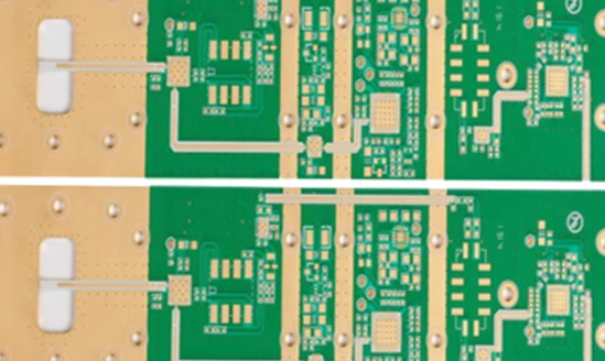
China Shenzhen KFPCBA Technology Co., Ltd. is a PCB design company specializing in electronic product circuit board design (layout wiring design). Mainly undertake multi-layer, high-density PCB design drawing board and circuit board design prototype production business. The PCB design team with an average of more than 10 years of work experience can skillfully use the mainstream PCB design software in the market, communicate professionally and efficiently to ensure the progress of PCB design, and help customers to seize the market opportunities quickly!

PCB design business areas:
| Communication product circuit board design services | GSM/GPRS, switches, RF equipment, etc. |
| Digital/Digital Product Circuit Board Design | Set-top boxes, HDTVs, digital cameras, camcorders, etc. |
| Security product circuit board design | Video surveillance, intercom, etc. |
| PC and related product circuit board design services | MB、NB、SERVER Motherboards and various industrial control boards, etc. |

PCB design needs to provide information:
1. Schematic diagram: a complete electronic document format that can generate the correct netlist;
2. Mechanical size: Provide the specific position and direction identification of the positioning device, as well as the identification of the specific height limit position area;
3. BOM list: mainly to determine and check the specified package information of the device on the schematic diagram;
4. Wiring Guide: Description of specific requirements for special signals, as well as design requirements for impedance, stacking, etc.
Our common software for PCB design:
Allegro, PADS, Protel, ORCAD, AD, PADS_LOGIC, etc.;
PS: We can convert the ORCAD format according to the PDF schematic diagram provided by the customer, and then import the netlist.
PCB design routine delivery:
The design cycle is as follows on the basis of the schematic diagram and the complete device package:
| layers | Design cycle |
|---|---|
| 2laminate | 2-3working day |
| 4laminate | 4-5working day |
| 6laminate | 6-7working day |
| 8laminate | 7-8working day |
| 10laminate | 10-12working day |
Consult now:
business phone:18825224069(Mr. Mao)
Business mailbox:[email protected]
-
No comment


 tel:+86-18825224069
 email:


