


 tel:+86-18825224069
 email:
 address:201, Factory 6, Longhui Industrial Park, Fuqiao 3rd District, Xinhe Community, Fuhai Street, Baoan District, Shenzhen china
Circuit Board Design And Production Process Preparation Steps
Release date:2022-12-29 15:52:49 Number of views:104
Circuit board design and production process Preparation of production materials Steps for preparing production materials
Shenzhen KFPCBA Electronics is a circuit board design and production manufacturer that can provide circuit board design, circuit board proofing, and PCBA OEM materials. It has a professional circuit board design team and its own PCB board factory . One-stop service saves you worry and effort !

Circuit board design and production process
1. Prepare production materials
The preparation of production materials is divided into two steps, including both the PCB designer and the engineering reviewer of the board factory.
First of all, regardless of whether the PCB design software is AD or PADS, when the design is completed and is about to be interactively produced, it is recommended to output the design file for data confidentiality and actual production needs.
It is the most common and common practice in the circuit board industry at present. One of the most common data formats for data is RS-274-X. Simply put, it is the industry standard.
From the perspective of PCB designers , the task is completed at this step. The next thing is handed over to the factory.
After the data is packaged and sent to the board factory, it will not be directly produced. After all, the board factory is also afraid that there will be a lot of problems in the customer's design, which will exceed their processing capabilities. For example, if the line spacing is too small, direct production is likely to be short-circuited. In case of a short circuit between the power supply and GND, the entire circuit board will spark with lightning after power on.
What to do, just throw the pot to the board factory.
Therefore, after receiving the customer's information, the board factory still needs to review the production materials, which is why the production cost includes the engineering cost.
The board factory usually uses it to review the data. (This software is mainly used by board factories. If an engineer wants to check his own circuit board design company , it is enough to learn one, and there is no need to learn it.)
Data review includes manufacturability inspection (line width, line spacing, solder mask bridge, silk screen, etc.), electrical performance inspection (IPC netlist comparison), and at the same time adjust the file according to the requirements of the customer and the factory's own situation ( Adjust line width or stackup, etc. according to impedance requirements).
The CAM review is completed, the data is offline, and the preliminary preparations have been completed here.
2. Circuit board manufacturing
The production and manufacturing of circuit boards is a complicated process. The general process of the whole process is as follows:
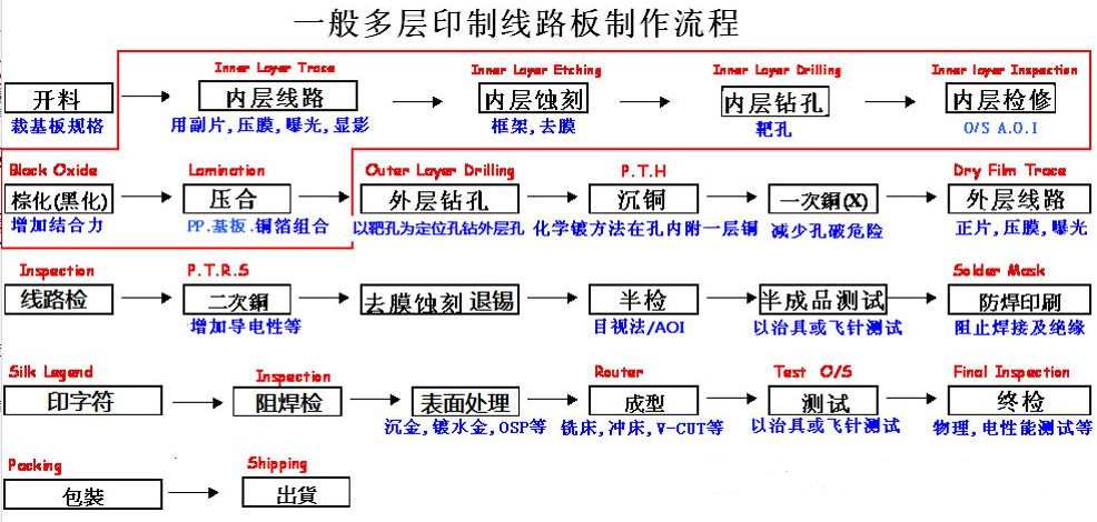
The picture above shows the production process of multi-layer boards. If it is a double-sided board, the part circled by the red wireframe will be missing. There are more than 20 steps in total. In order to facilitate everyone's understanding, we simplify the process and only list the key steps.
1. Copper-clad boards are dried and cut into small pieces for production;
2. Corrosion of the inner circuit;
3. Pressing, so that the substrate and copper foil are combined;
4. Drill holes, and then sink copper on the holes to make the vias have electrical properties;
5. Make the outer circuit;
6. Secondary copper to increase conductivity;
7. Apply green oil (black oil, white oil, red oil, colorful oil);
8. Screen printing;
9. Surface treatment;
10. Forming (V-CUT, etc.);
11. Test (flying probe test, impedance test, metallographic section analysis, etc.);
There are so many simplified processes, but it does not mean that the steps not introduced are not important. In the actual production process, every step has its necessity. In order to catch up with efficiency, some board factories will compress some steps, such as reducing the time of high-temperature baking or not baking at all, which will cause some boards to have copper skin blistering and cracking during welding.
3. Production and design
The production of PCB is in the factory, and there are not many opportunities for many circuit design engineers to get in touch. But a general understanding of PCB manufacturing and a reasonable estimate of possible problems in the production process can make the design more reliable.
Let me give a few small examples to illustrate:
1. Since the circuit is formed by etching, the actual line width will have an error from the ideal value. Usually the line width is ±1mil below 10mil, and the line width is ±10% above 10mi. At the same time, the etching factor will also affect the upper and lower line widths of the traces. Therefore, when calculating the impedance, the upper line width of the outer layer is about 1 mil smaller than the lower line width, and the value of the inner layer is about 0.5 mil.
2. Although the multi-layer board has rake holes for alignment, there are still errors during lamination, so layer deviation will be formed, and the layer deviation can reach 3mil in some extreme cases. This may cause the traces of the upper and lower layers to overlap, or deviate from the reference plane.
3. There are two mainstream production methods of silk screen printing, one is inkjet and the other is printing by making screen. For the latter, the position of silk screen printing will have a large error. This is why precise positioning cannot be done by silk screen printing.
Every link of manufacturing may affect the performance of the circuit, and there are too many things involved.
Why choose Shenzhen KFPCBA to do circuit board design and production?
1. Strength Guarantee
▪ SMT workshop: It has imported placement machines and multiple optical inspection equipment, with a daily output of 4 million points. Each process is equipped with QC personnel, who can keep an eye on product quality.
▪DIP production line: There are two sets of wave soldering, among which there are more than ten old employees who have worked for more than three years. The workers are highly skilled and can weld various plug-in materials.
2. Quality assurance, high cost performance
▪High-end equipment can be attached to precision special-shaped parts, BGA, QFN, and 0201 materials. It can also be used as a sample patch, and bulk materials can be placed by hand.
▪Prototypes and large and small batches can be produced, starting from 800 yuan for proofing, 0.008 yuan per point for batches, and no start-up fee.
3. Rich experience in patching and welding of electronic products, stable delivery
▪Cumulatively serve thousands of electronic companies, involving SMT patch processing services for various types of automotive equipment and industrial control motherboards. Products are often exported to Europe and the United States, and the quality can be affirmed by new and old customers.
▪On-time delivery, normally 3-5 days after the materials are complete, and small batches can also be shipped on the same day in an expedited manner.
4. Strong maintenance ability and perfect after-sales service
▪Maintenance engineers have rich experience in Shenzhen circuit board design company , can repair all kinds of bad products caused by patch welding, and can ensure the connection rate of each circuit board.
▪24-hour customer service personnel respond at any time to solve your order problems as quickly as possible.
Shenzhen KFPCBA recommended service:
related articles:
Comment on this article here
-
No comment

Ripple
Hi everyone, I'm Ripple, Sales Director of KFPCBA Tech Ltd. If you are looking for a one-stop PCB and PCB assembly manufacturer in China, KFPCBA is your best choice! Please feel free to contact our team! Thanks!
Contact me now


