 address:201, Factory 6, Longhui Industrial Park, Fuqiao 3rd District, Xinhe Community, Fuhai Street, Baoan District, Shenzhen china
PCB Process Edge Is Very Important For The Subsequent SMT Patch Processing
The reservation of the PCB process edge is very important for the subsequent SMT patch processing
In the PCB production process, there is one more important process, that is, the process edge, and the reservation of the process edge is extremely important for the subsequent SMT patch processing . Next, the Shanghai PCBA processing factory will introduce the function, production method and design requirements of the PCB process side.
The role of PCB process side
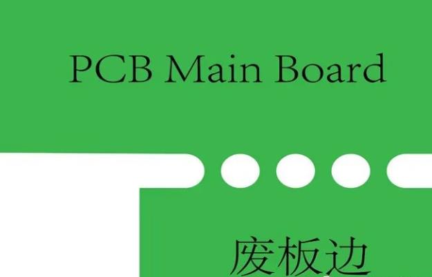
The process side is the part lowered on both sides or four sides of the PCB board, mainly to assist the soldering of the SMT plug-in to move the board, that is, to facilitate the track of the SMT placement machine to catch the PCB board and flow through the placement machine. If it is too tight When the components near the track are picked up by the nozzle of the SMT placement machine and mounted on the PCB, collisions may occur, making it difficult to complete production. Therefore, a certain process edge must be reserved, usually with a length of 2-5mm etc. These methods are also applicable to the design and manufacture of some plug-in component components to avoid similar phenomena during wave soldering.

The process edge is not part of the PCB board and can be eliminated after the PCBA manufacturing is completed.

Manufacturing form of PCB process side
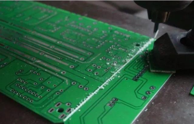
1. V-CUT: A kind of process connection between the process edge and the board. Cut the pcb design and production on both sides of the PCB board, but do not cut!
2. Connecting ribs: Use several ribs to connect the PCB board, and punch some postage holes in the middle, so that it can be broken by hand or washed by machine.


Design requirements of PCB process side
Not all PCB boards need to be processed. If there is a large space on the PCB and no SMD devices are placed within 5mm on both sides of the PCB, there is no need to add a process edge in these cases. There is another situation. There are no SMD devices within 5mm on both sides of the pcb board, as long as the process edges are processed on the other two sides, this requires the attention of PCB engineers.

The thin plate consumed by the process side will reduce the overall cost of the PCB, so when designing the PCB process side, it is necessary to balance economy and manufacturability.
For some special-shaped PCB boards, the original PCB board with 2 process sides or 4 process sides can be greatly simplified through the jigsaw form.When designing the jigsaw form during SMT processing, it is necessary to fully consider the track length of the SMT placement machine, and it is not necessary to communicate with the process engineer of the SMT supplier for the jigsaw board with a length of more than 350mm.
-
No comment


 tel:+86-18825224069
 email:


